This page describes a shielding electrode for HVDC GIS insulators with the aim to reduce insulator surface charges for fluid filled or dry-type GIS cable terminations.
How to geometrically shield an epoxy at the edge of the insulator to significantly increase flash over withstand for HVDC application.
To prevent this a specific shielding electrode geometry can be implemented at the top of an insulator, this will decrease the electrical stress at the insulator edge and significantly reduce the risk of interface discharge to occur. In the example here, the insulator is made of epoxy, but it could be of another material or a variation regarding the material or the thermal and/or electrical conductivity of the insulator.
The technical solution is found in the shielding profile and positioning towards cable termination and the switchgear main circuit end terminal. The two design points are:
- A larger outer diameter of the shielding electrode than the cable termination insulator top part outer diameter, which should be in the range difference of 0.1-200 mm. Preferably with large radius to limit E field in the enclosure insulating medium. Since the insulator is conical and will exceed diameter at some point along the entire interface length to ground, the top of the insulator can be clarified to be, but not limited to, 0.1-500 mm of the epoxy insulator.
- The shielding electrode Position very close to the insulator 0.1-50 mm, but no direct contact between the insulator top and shielding electrode.
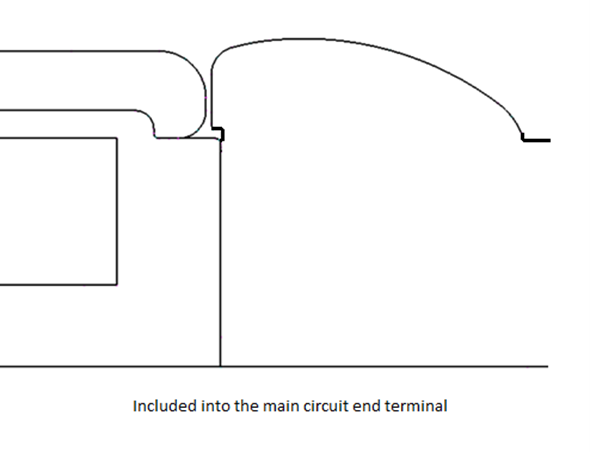
This can be achieved either as (1) an adapter, (2) incorporated into metallic insert of insulator or (3) incorporated the main circuit end terminal.
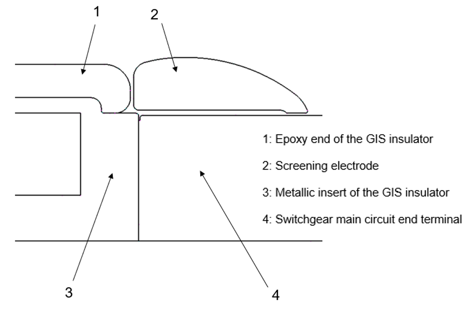
1: Epoxy end of the GIS insulator. 2: Screening electrode. 3: Metallic insert of the GIS insulator. 4: Switchgear main circuit end terminal
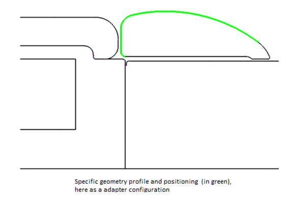
Specific geometry profile and positioning (in green), here as an adapter configuration
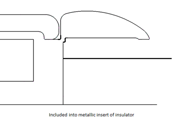
Included into metallic insert of insulator